Quality comes first in PCBs!
To guarantee the respect of the specs and of the building characteristics of PCBs according to requirements and more and more restrictive quality standards, it is necessary to equip the laboratories of the PCB manufacturing and trading companies with instruments capable to support the statistical process control and the analysis of the PCBs manufactured trough these processes, starting from the constitutive base materials.
To grant the quality of PCBs of increasing complexity and technological content all along their life cycle became a "must” for OEM active in all marketing sectors from Aerospace & Defence to Automotive and nevertheless in Rail, Medical and Industrial Automation sectors.
The process of miniaturization together with the new coming needs of PCB consumers in terms of performances of the finished electronic equipment had the cumulated effect to increase the complexity of PCBs and, as a consequence, forced to adopt the most advanced technologies to ascertain PCB conformity both, according to the international standards and according to specific requirements coming from the final customer.
The international standards, the IPC norms before all, suggest, in particular, to improve the interaction among the PCB designers – represented by the final customer in the most of the cases -, the PCB manufacturers and the PCB assembly service companies in order to reduce the criticalities of the PCBA (Assembled PCB) and, more in general, of the finished product.
The test methods to validate the conformity of PCBs are described by the IPC TM650 and by different and additional norms related to specific sectors like the MIL for the Military sector and the ESA ECSS for applications in the Space sector.
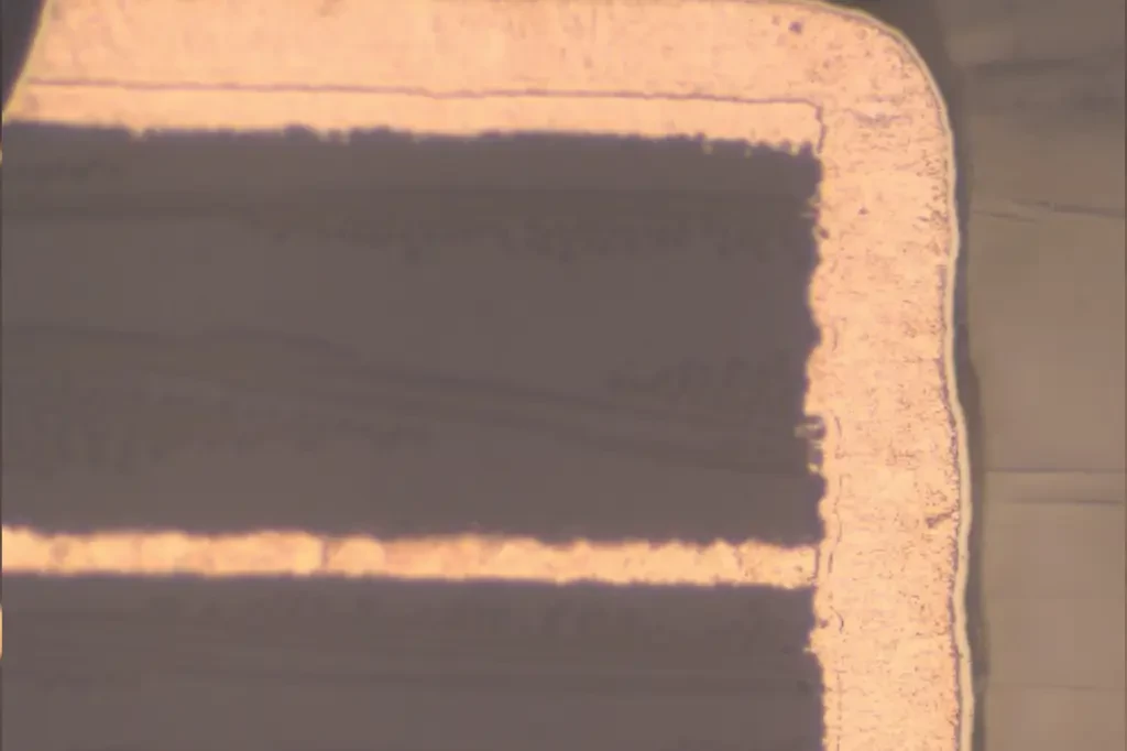
The way to prepare and to "read” cross sections are also described by the IPC.
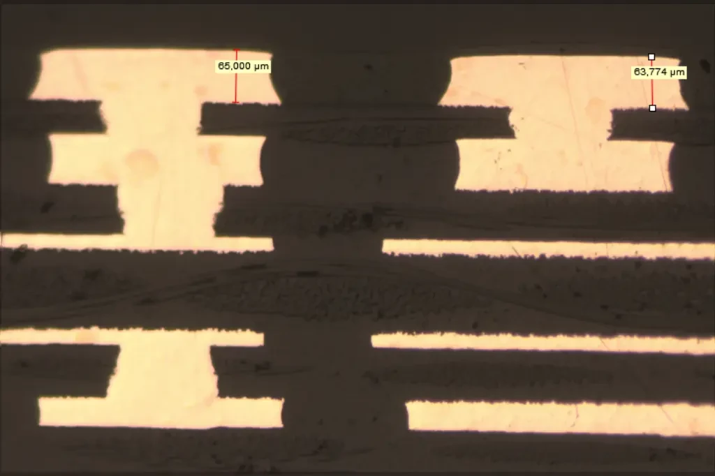
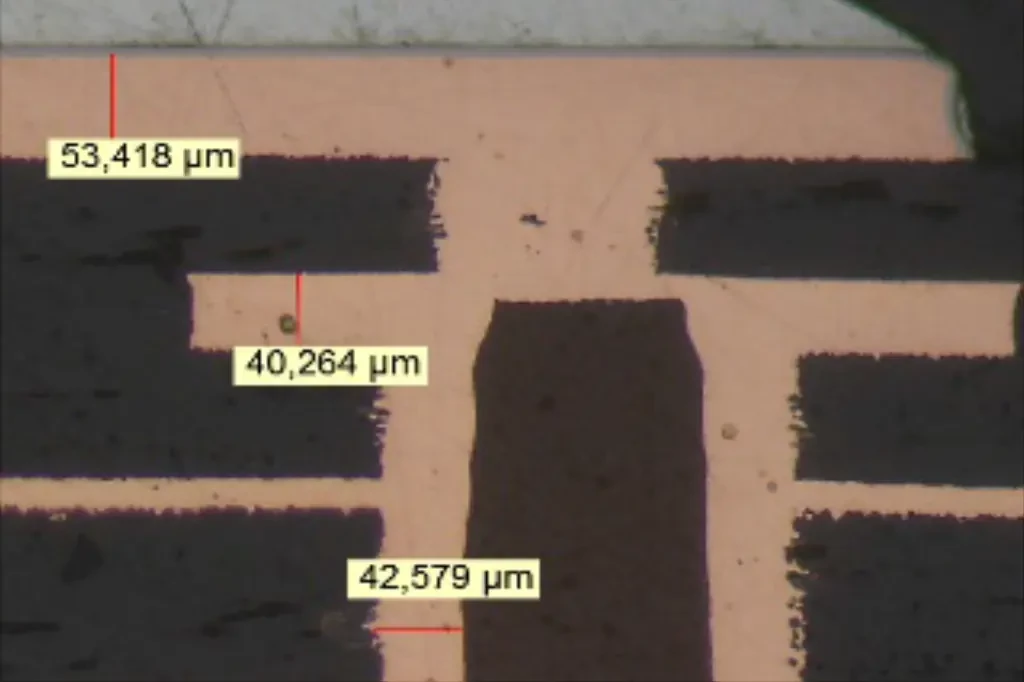
Microsections are adopted to check the internal characteristics of PCBs (i.e copper plating thickness, quality of copper filling for blind vias, quality of resin filled vias in case of via in pad solutions in particular) and for the evaluation of the most critical points like the corners of PTH holes and vias or of the annular ring in where inner layers are drilled so to be connected to each other.
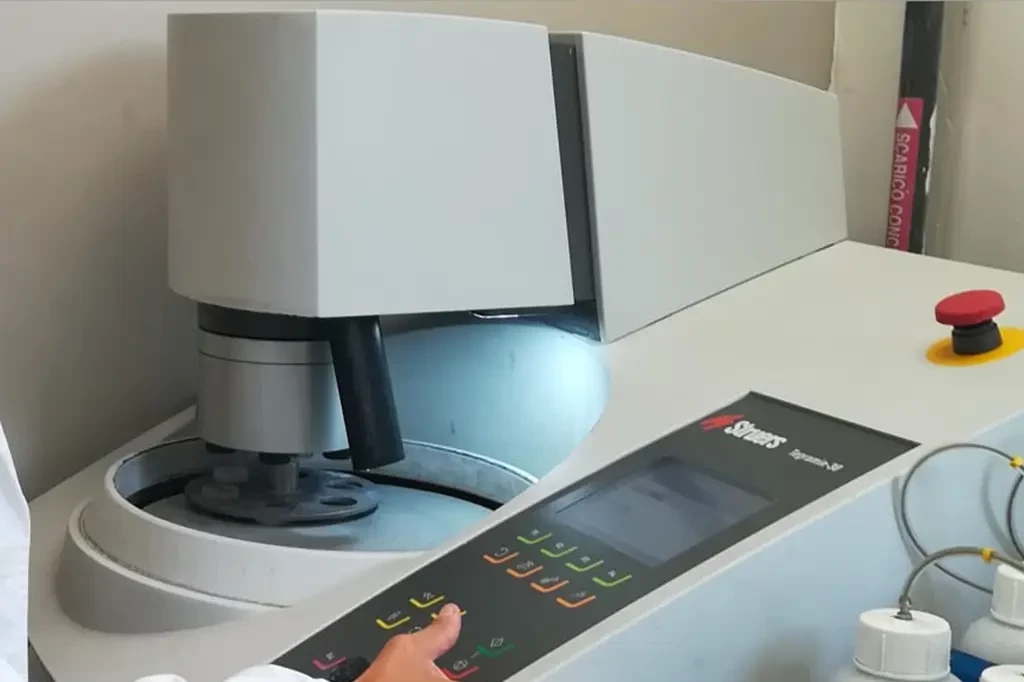
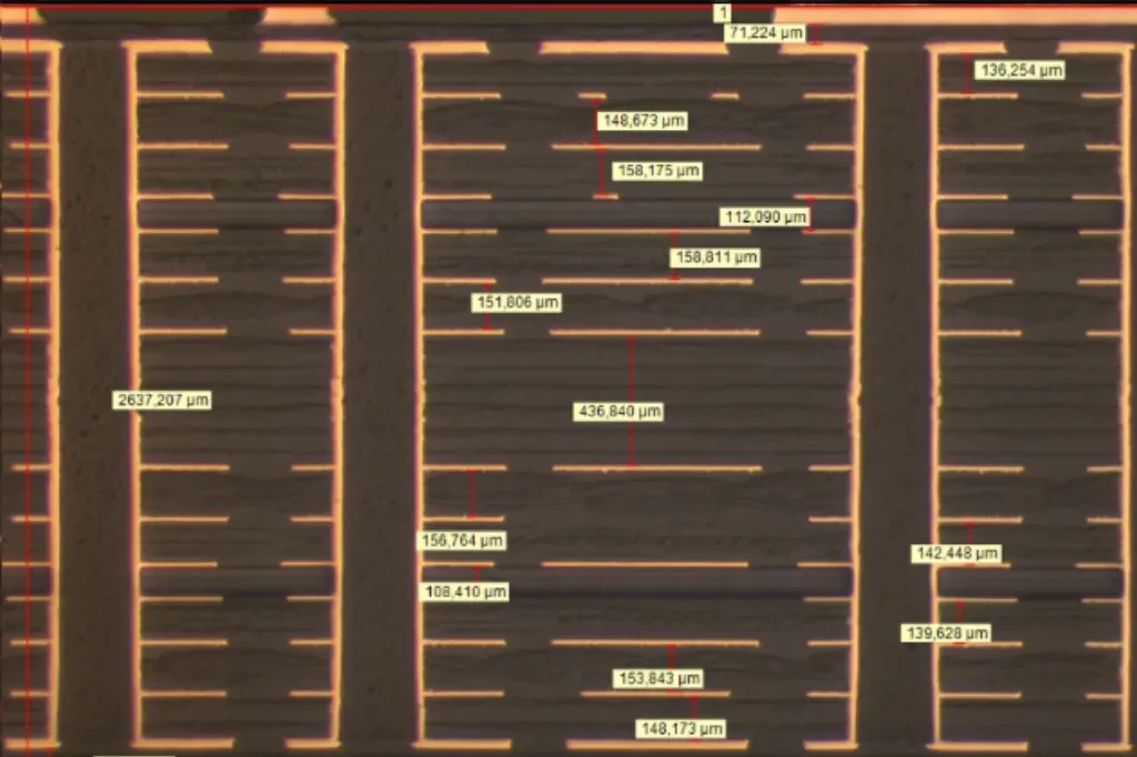
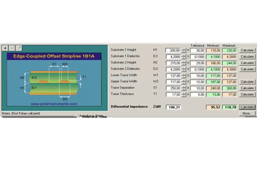
Another important aspect is the verification of correctness of the stack up, mainly, but not only, for PCBs with nets with controlled impedance. With microsections is possible to evaluate the presence and the thickness of each and every layer, and, even more, to evaluate thickness of base copper of the inner layers and of the successive platings with chemical copper and electrolytic copper.
The controlled impedance are calculated in the PCB design phase on the basis of the selected base material to produce it, and then will be rechecked and simulated in feasibility analysis and engineering phase by the PCB manufacturer on the basis of the definitive material agreed by the designer and the PCB manufacturer.
The dielectric constant of the insulating material – pre-preg and core of inner layers - together with the section size of the nets determine the value of controlled impedance of nets.
Is possible to check the value of controlled impedance trough specific test coupons designed on the PCB production panel and therefore manufactured together with the PCB.
The necessity to reduce the PCB size forced the PCB designers to increase the number of internal interconnections between layers and to adopt more complex technological solutions like blind vias, single and sequential, stacked or staggered, blind vias and buried vias.
More complex structures with increased drill’s density make the internal structure of PCBs more sensible to thermal stresses related to the soldering process where two options, or a combination of them, are possible: wave soldering process for TH components or SMD soldering process for SMD components.
For this reason, the thermal stress tests are important to simulate the behaviours of PCBs and their robustness during the soldering process of the electronic components on them.
Thermal stresses are executed in order to check and validate the quality of copper plating of PTH holes according to two possible options: 3 thermal stresses at a 288°C (IPC TM 650 2.6) or 6 stress a 260°C (IPC TM650 2.6.27).
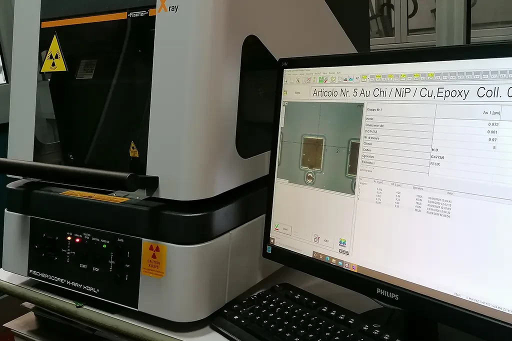
In addition to the destructive analysis, so those that force to destroy and waste the PCBs, that are often necessary to investigate the internal characteristics of the PCBs coming from the special processes involved in the PCB manufacturing process, not destructive analysis are performed like the X-Ray Fluorescence Spectroscopy (XRF) to determine the thickness of the PCB finishes (HASL, ENIG, ENEPIG, tin-lead Hot Oil reflow, Immersion Silver, Immersion Tin, iSiG,- Hard Gold).
The analysis of the thickness of the finishes, are not only important to control the process, but they are necessary to prove the conformity of the boards. Not conformity of the thickness of the finishes could, in fact, generate quality problems of electronic components soldering.
Through the contaminometer is also possible to determine the ionic contamination on the PCB surface, on the finishes and on soldermask. This method is known as Resistivity of Solvent Extract (ROSE) and is performed with the aim to detect excess of halides on PCB surface that could generate soldering defects and weak adhesion of conformal coating.
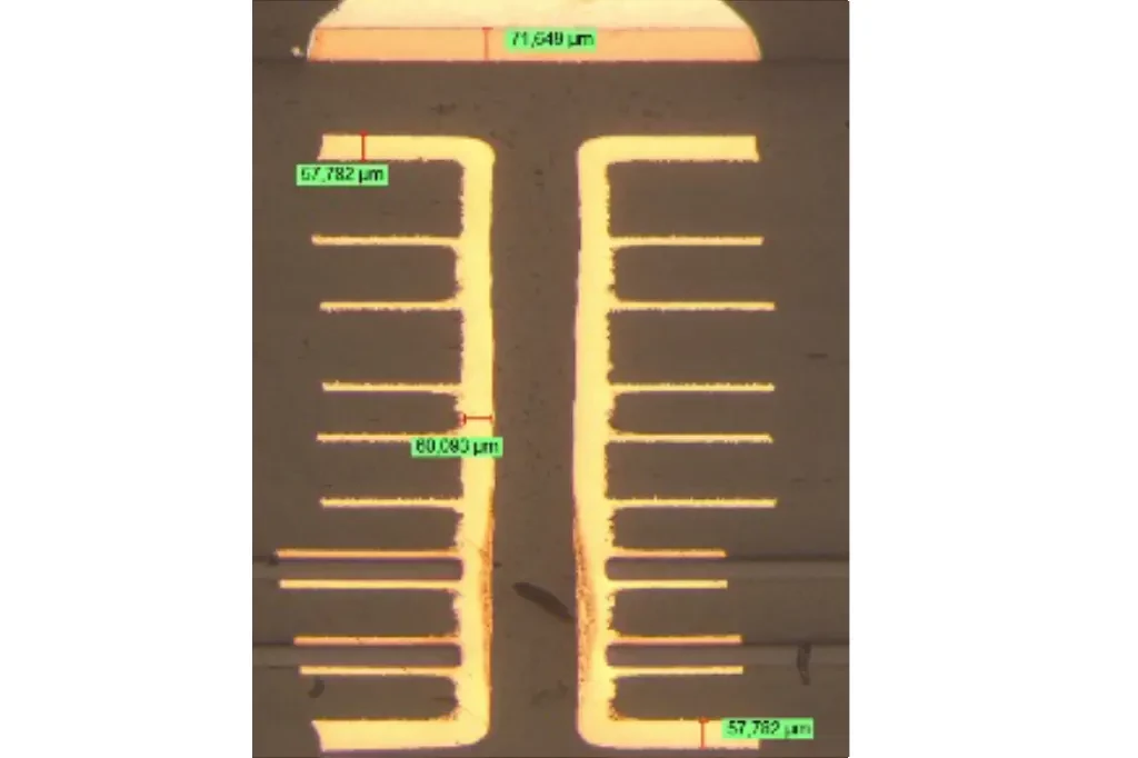
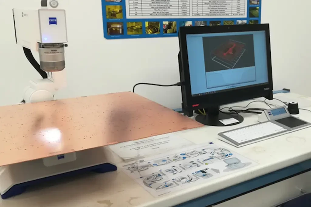
Moreover, the most recent 3D microscope technologies for inspection allowed to substitute not destructive analysis to destructive ones i.e. to check surface roughness, dimple of filled holes, cavity depth, etching value for RF nets, and for quality verification of laser and mechanical drilled blind vias, back drilled vias included.
This technology allows to significantly reduce the time needed to test and validate the quality of PCBs.
The whole of the aforementioned analysis, together with some additional ones that will be the subject of another short tutorial, grant the conformity of the PCB and its stability during the time.
The results of these analysis are collected in the most common reports adopted to certificate the conformity of products like the FAI Report, the PPAP and the Test Report prepared and filled according to the EN9100, IATF, ISO13485, ISO TS 22163 and ESA ECSS standards and to different/additional requirements coming from customers.
Cistelaier, TECHCI and EPN Electroprint – the three companies of the PCB Division of the Finmasi Group – grant the quality of PCBs through the best available inspection and test technologies.