Moisture, an invisibile enemy for PCB and PCBa integrity
When the RoHS regulation started in year 2006, the Tin-Lead based soldering pastes have been substituted by Lead free pastes.
Excepted for a few cases, represented by the applications for the Military field, for the Space sector and for the security parts for Automotive purpose, the Lead free pastes replaced the Lead based pastes for the soldering of electronic components on PCBs.
This transaction implied an increase of soldering temperatures of about 30-40 °C with the effect to show effects on the PCBs’ and PCBAs’ conformity that before that moment were considered of minor relevance or marginal interests, like that due to moisture evaporation.
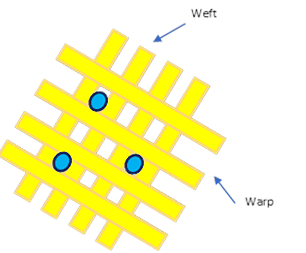
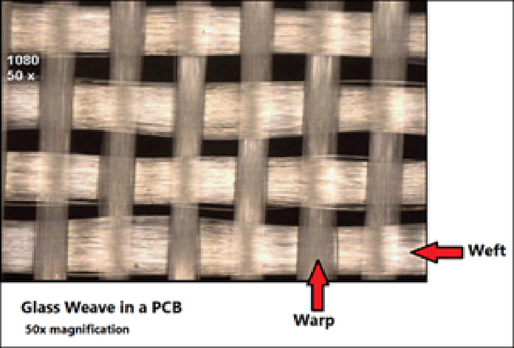
The standard base materials are made of glass fibre tissue (weft and warp) pre-impregnated with epoxy resin. The resin makes the bulk highly hygroscopic, and so easily capable to absorb moisture present in the local environment.
The presence of moisture inside the PCBs became an aspect to keep in due consideration after the transaction from Lead based to Lead free soldering pastes.
As it is possible to see in the following pictures, the moisture, in the form of micro-particles of water vapour creeps between the glass fibres drown in the epoxy resin.
If this condition was of none risk in the past, with the implementation of the Lead Free technology brought at light a lot of criticalities.

As it is possible to see in the graphic here following, the pressure typically generated during the soldering process for the assembly of electronic components on PCBs, raises from 400 PSI in case of Lead based soldering pastes up to 600 PSI in case of Lead free pastes. This means that the increase of soldering temperatures have the consequence of increasing the pressure inside the PCBs during PCBAs’ soldering phase.
Therefore, the presence of moisture in PCBs could generate the "delamination” phenomenon during the PCBAs’ soldering phase.
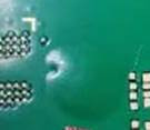
Delamination is one of the most critical defects for PCBs. It consists in the separation of the base materials involved in the build-up structure of a PCB. The typical appearance is an evident bulging on the surface of the PCB.
This phenomenon prejudices the functionality of the PCB as an effect of lack of insulation between different layers of the PCB itself or due to the metallized hole breaking, both, in case of vias or case of PTH.

An important aspect to keep in due consideration is related to the configuration of the PCB and to its constructive characteristics.
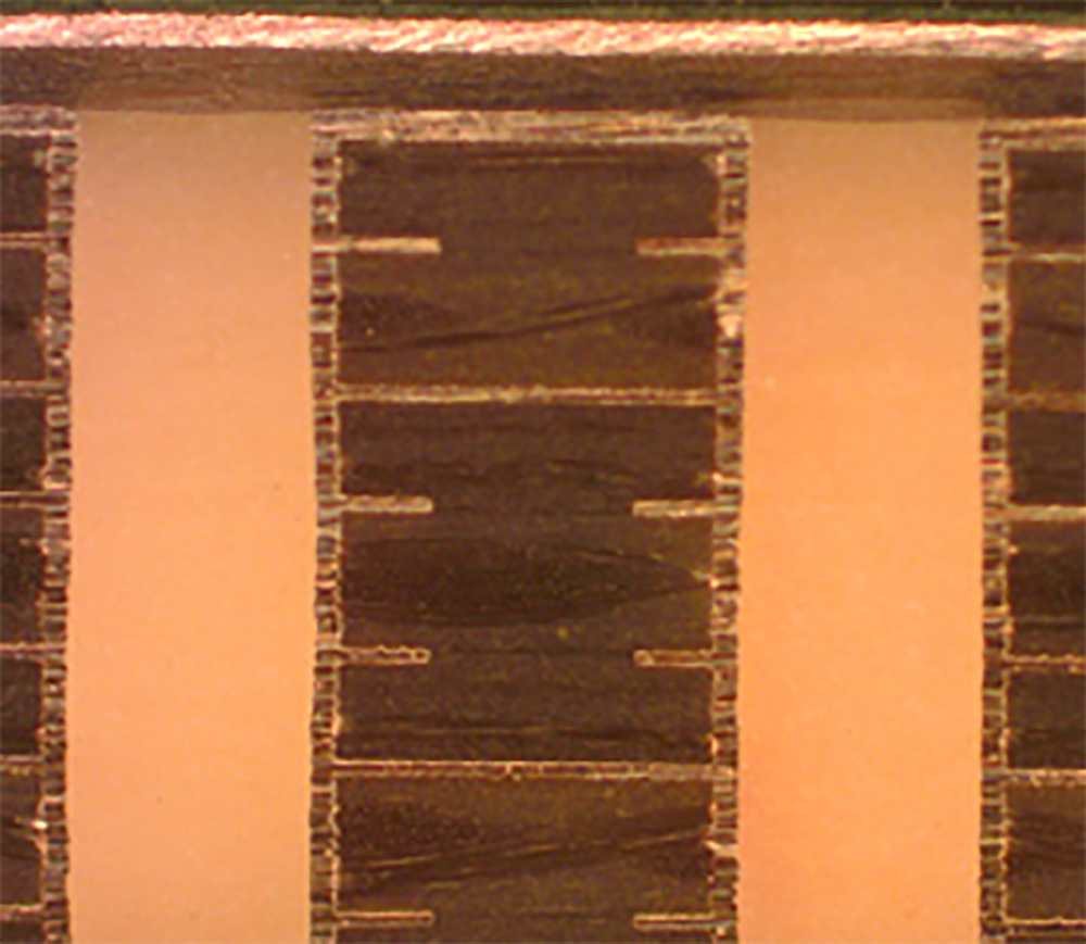
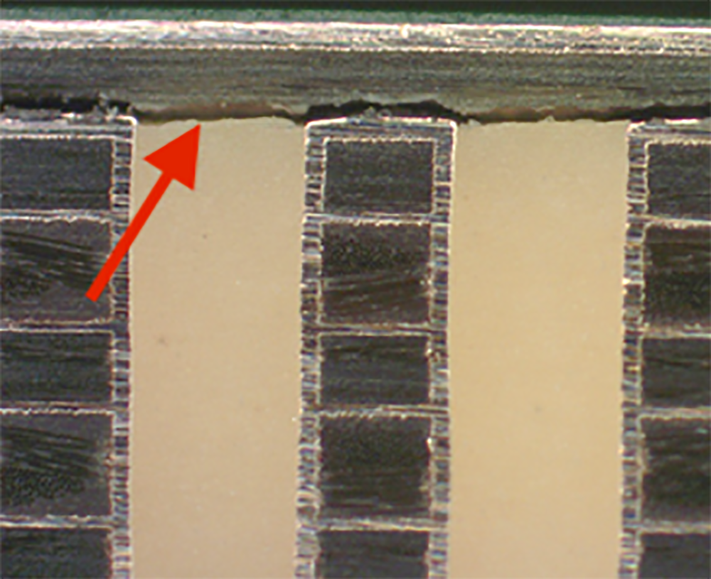
Type VII vias’ filling technology according to IPC 4761 based on vias’ filling with thermo-conductive resin is a tipical example: this resin is, in fact, highly hygroscopic and therefore represents a bulk in which moisture could remain trapped and that later on, due to soldering temperature, will "try” to exit the PCB generating delamination, as it is possible to see in the images here below.
For this reason, the PCB baking in oven before soldering is necessary to prevent situations that could prejudice the PCB conformity.
Moisture in PCBs could be responsible not only for delamination during the assembly process but could promote copper pads oxidation and, consequently, could reduce the surface wetting characteristics necessary to get a good surface finishing.
In the next article we will explain additional phenomena related to moisture and related countermeasures suggested by the international standard of IPC 1601.