IPC-2226 Standard for HDI PCB Board Design
With this article and some others that will follow later we would like to share available knowledge in the PCB design and manufacturing field.
Following some articles related to HDI PCBs we would like to describe the three related more common build-up structures.
HDI PCB types
The design designation system of this standard recognizes industry approved design types used in the manufacture of HDI printed boards. The designations determine the HDI design type by defining the number and location of HDI layers that may or may not be combined with a substrate.
Type I, Standard build-up for HDI
This construction describes an HDI in which there are both blind vias and through vias used for interconnection. Type I constructions describe the fabrication of a single blind via layer on either one or both sides of an PCB substrate core.
 Type I structure
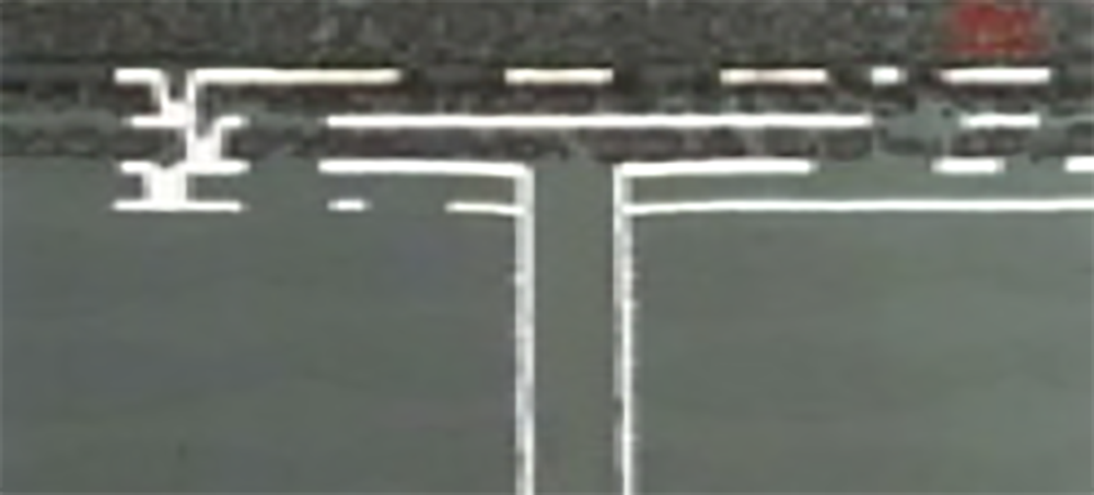
 Laser blind via
The PCB substrate is typically manufactured using conventional PCB techniques and laser via hole technology. The substrate can have as few as one circuit layer or may be as complex as any number of inner layers. (see the picture here following)
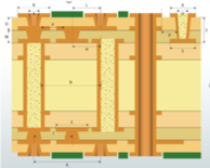
Type II, Sequential build-up 1+N+1
Tipe II is characterized by buried vias in the core and may have through vias through the outer layers. Type II constructions describe an HDI board in which there are plated microvias, plated buried vias and may have PTHs used for surface-to-surface interconnection.
Microvias on layer 1 and layer n grant the connection to conductors on layer 2 and layer n-1, making the connection with the core. Type II constructions can also have PTH to connect layer 1 directly to layer n. (see picture here following)
 Type II structure
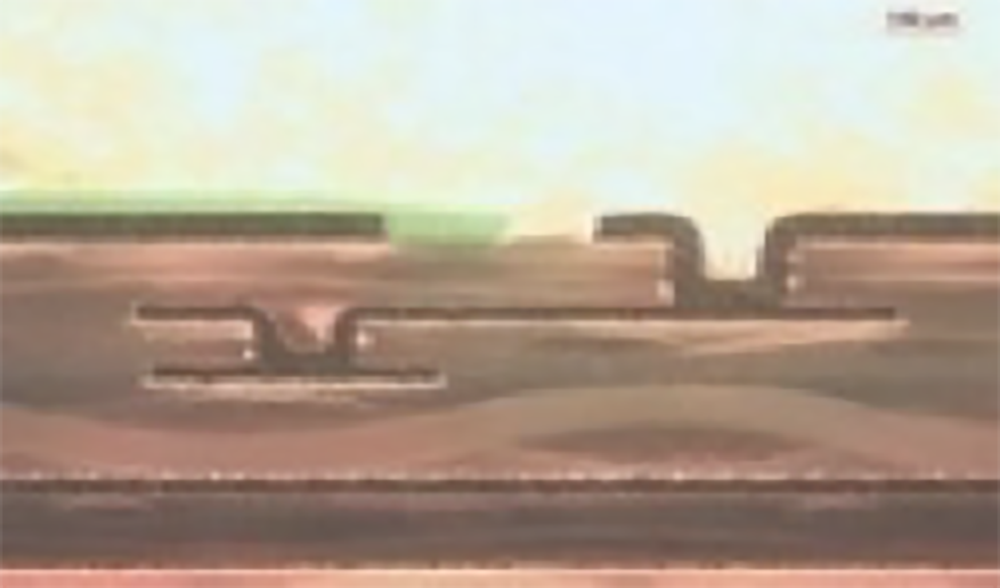
The buried vias may be prefilled with a conductive or nonconductive paste or, partially or completely, filled with dielectric material from the lamination process.
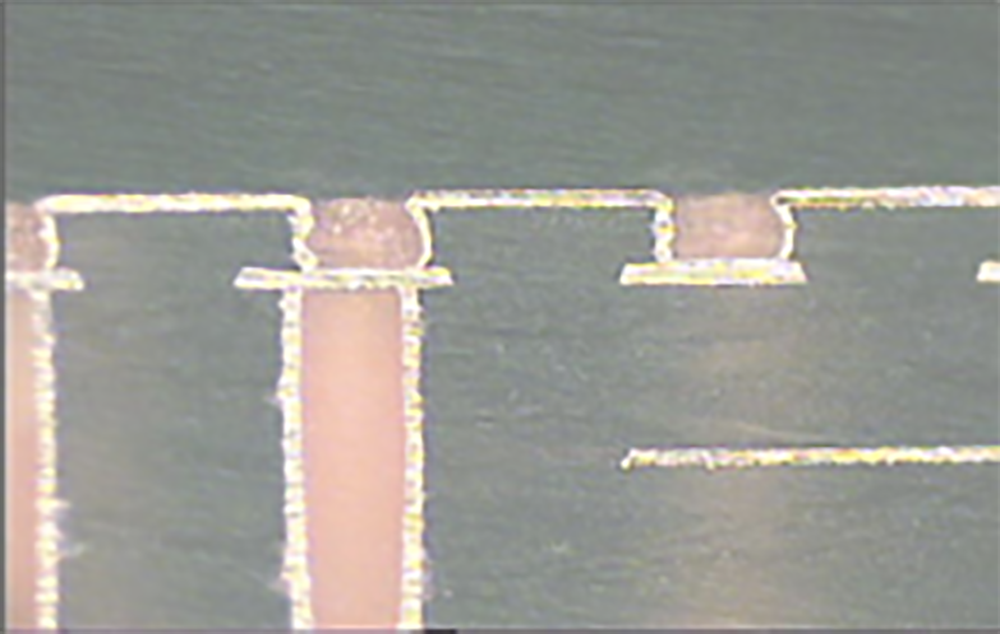
The below figures show two buried vias in the core substrate formed prior to applying the HDI dielectric layers. Both vias connect layer 2 to layer n-1. The via on the left is filled with pre-preg resin. The via on the right is filled (& capped) with a not conductive paste: in this way is possible to laser drill over the pads that is plated so to gain space for the design.
Struttura Tipo III, build-up sequenziale X+N+X
Type III constructions describe an HDI in which there are plated microvias, paste/resin filled holes and through vias used for interconnection. Type III constructions are distinguished by having at least two microvia layers on at least one side of a substrate core. The substrate core is usually manufactured using conventional PCB techniques, may be rigid or flexible, and have as few as one or as many as any number of layers with buried vias. (see picture here following)
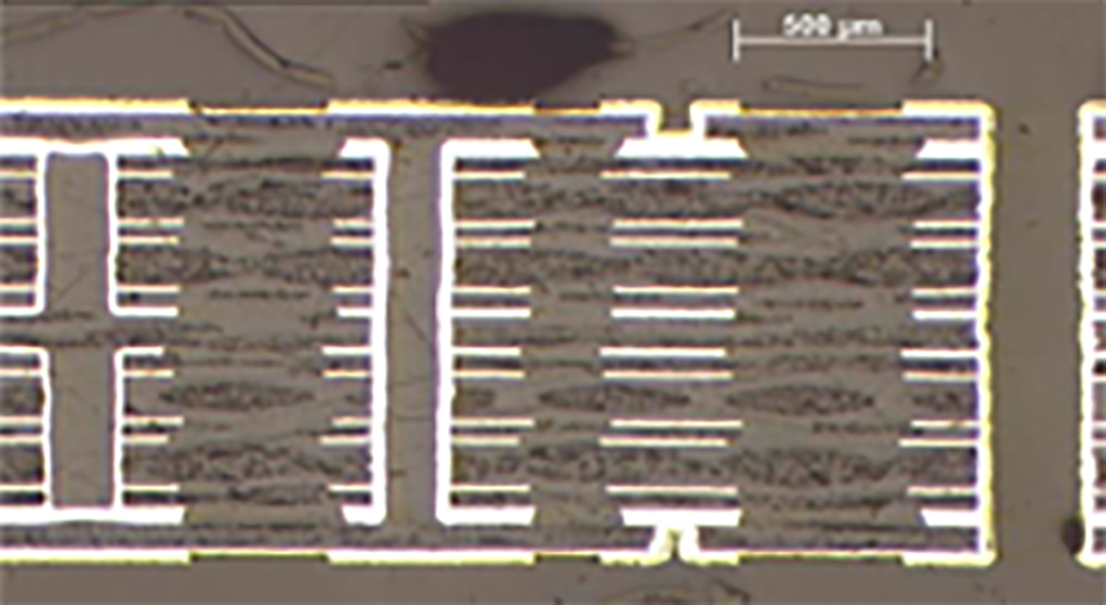
Where space is minimal and if expressly requested, stacked vias - stacked blind holes - must be used - while where conditions allow it, staggered vias - non-overlapping blind holes on several levels - can be used. Staggered vias are less critical, so preferable, for manufacturing than stacked vias. (here following some pictures coming from microsections)