Surface finishing for PCBs: Let’s go into detail!

As explained in the previous article, for Printed Circuit Board (PCB) manufacturing surface finishes technologies have a crucial role in electronic components assembling.
Each surface finishing has specific characteristics, which mark pros and cons and, referring to cons, right tricks and precautions can be taken during PCB manufacturing.
Let’s go into detail of the most common surface finishes.
HASL Lead Free-HASL Sn/Pb [Normative Reference IPC-6012]
PCB is immersed in a bath of molten tin and then hit by high-pressure hot air jets that flatten the thickness and remove the excess from holes and pads.Thickness varies from 1 to 45 µm and is influenced by pad geometry, for this reason it is not particularly suggested for HDI PCB with VFP (Very Fine Pitch) and BGA (Ball Grid Array). This finish is not suggested for flex and rigid-flex PCBs since thermic and mechanical stress coming from process air jets could damage the boards.This type of finishing is particularly suggested for multiple soldering cycles and for long storages since tin alloy is characterized by longer Shelf Life.
ENIG [Normative Reference IPC-4552]
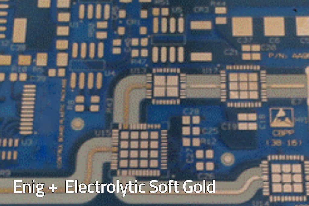
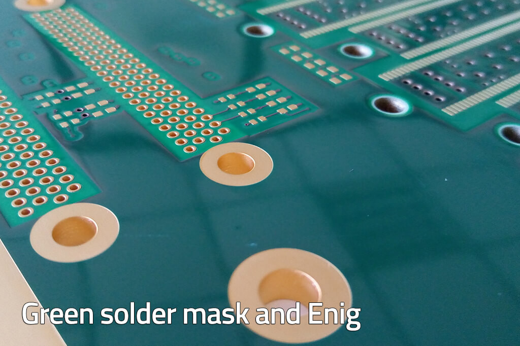
Chemical process which plates the exposed copper with Nickel and Gold. Nickel thicknesses are usually 3-6 µm, while for Gold the minimum thickness is 0.05 µm as provided in the normative reference.This chemical finish, differently from HASL, is particularly suggested for HDI PCB with VFP and BGA, since coating planarity and homogeneity are granted. These characteristics make this finish suitable also for press-fit technology for which it is really important holes’ diameter tolerance respect.
Immersion TIN [Normative Reference IPC-4554]
Immersion Tin, more commonly named Chemical Tin, is a surface finishing, which has begun to be widely adopted from the beginning of year 2000, mainly sponsored in Automotive sector attracted to the chance to have an automatic horizontal process with tin planarity coating, differently from HASL.
This surface finishing results critical for the handling and is particularly sensitive to storage conditions; therefore, is strongly recommended to assemble PCB with this finishing within 3 months from manufacturing date to have an optimal operative window. Is not particularly indicated for multiple assembling given the thin copper thickness (0.8-1 µm) and given that at each soldering step the surface intermetallic layer increases, limiting the weldability.For this kind of finishing is fundamental the vias treatment, is necessary to plug holes or to keep them completely open to avoid issue such as Acid Traps and consequent risk of delayed hole dismetallization.

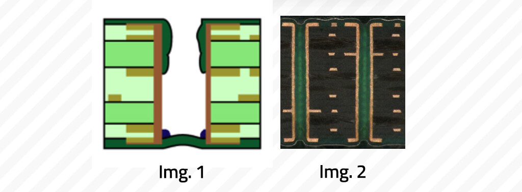
IPC4761, guideline for vias treatment, suggests a Tenting double side or complete Pluggin (Image 2) for this kind of finishing, to avoid that finishing residues could be trapped inside the holes (Image 1) with the consequence to experience corrosion of hole walls through time.
Immersion Silver [Normative Reference IPC-4553]
Realized by a chemical process of immersion through which a Silver layer with variable thickness between 0,2 and 0,4 µm would be deposited. Silver finishing, due to thickness, is particularly suitable for technologies where planarity is fundamental such as VFP-BGA-Press-Fit. Differently form Chemical Tin, it has longer Shelf Life, 6 months more or less, and finishing Rework process is easier. An important feature of this finishing is packaging through which the manufacturer packs the PCBs; is very important that the paper inserted between PCBs is Sulphur free to avoid contamination of Silver on the surface.
OSP [Normative Reference IPC-6012]
OSP is an organic compound that selectively bonds with copper so to plate copper itself, providing an organic-metallic layer. Thickness, measured in A° (angstrom), protects it until soldering. OSP is the surface finishing most used in the world, particularly in white industry due to low costs and easy-to-use. Shelf life is limited, therefore is suggested to assemble PCBs within one month, but the chance to redo finishing on stored pieces makes it suitable for long storage necessities. Standard OSP process doesn’t fit multiple soldering while OSP HT could support it.

HARD GOLD [Normative Reference IPC-4552]
Hard Gold finishing is composed by Nickel (3-6 µm) and Gold (0,8-1,2 µm), and it is realized through electrolytic galvanic process, that allows the finishing to plate copper. Gold high thickness makes this selective finishing suitable for interference solutions (PCB with insertion connectors) but not suitable to soldering, even considering the high related costs.
ENEPIG [Normative Reference IPC-4556]
ENEPIG finishing is composed by Nickel (3-7 µm), Palladium (0,05-0,25 µm) and Gold (0,02-0,05 µm), and it is realized through an immersion chemical process, that allows the finishing to plate copper. ENEPIG was born as an updated version of ENIG, with the addition of a Palladium layer between Nickel and Gold. Palladium layer plays the role of barrier to avoid Gold migration to Nickel layer, and of Nickel layer covering for the following Gold deposit reducing Nickel Spikes effect. Moreover, ENEPIG offers high reliable Wire Bonding capacity.
HOT OIL REFLOW [Normative Reference ECSS]
Hot Oil Reflow is a finishing usually used for SPACE products; it is indeed the only ESA (European Space Agency) approved surface finishing. It consists in re-melting, with high-temperature oil bath, the Tin-Lead electrolytically deposited on surface. This finishing grants good coating planarity, usually 5-7 µm tin on surface, and limited thermal shock to base material. Hot Oil Reflow technology, largely diffuse in ‘80s/’90s, isn’t use anymore except from who, such as Cistelaier, works in Space Sector.

In surface finishing’ choice, you need to evaluate its Shelf Life, meaning the operative window which grants the finishing to have a complete PCB weldability. Finishing Shelf Life is strongly influenced by PCBs packaging and storage. Is really important to pursue the right storage methodology (suggested by IPC-1601 guidelines) to preserve weldability and reliability, because of the high hygroscopic nature of the base materials with which PCBs are manufactured.
The following table shows typical Shelf Life and suggested ones to have a larger operative window and better performances of the surface finishing.
| FINITURA | SHEL LIFE | SHEL LIFE | Possibilità |
| Consigliata | Consigliata | di Rework | |
| HASL LF-SnPb | 12 Months | 12 Months | YES |
| ENIG | 12 Months | 6 Months | NO* |
| Im Tin | 6 Months | 3 Months | YES** |
| IM AG | 6 Months | 3 Months | YES |
| OSP | 3 Months | 1 Month | YES |
| ENEPIG | 6 Months | 6 Months | NO* |
| HOT OIL REFLOW | 12 Months | 6 Months | NO |
* For ENIG and ENEPIG finishing a reactivation cycle to improve surface wettability and shelf life is available.
** Chemical Tin rework not suggested